Showing posts with label graphene. Show all posts

Tuesday, 5 October 2010

From Nanotubes to Nanosheets: The New Horizon of Graphene Chemistry

Carbon nanotubes are cousins of graphite, diamond, and fullerene C-60. The chemistry of these tubular structures has been more or less established, since their discovery and more intensely over the past decade, mostly according to the existing knowledge of those other carbon allotropes. Among the chemistries being explored, those rendering the nanotubes soluble were of special interest, since they opened up a whole new playground to process these materials and to maximize their magic properties for applications.

Carbon nanotubes may be viewed as rolling up of single pieces of graphenes. To physicists, the tubular structure itself is interesting; moreover, the "opened" ones - the "nanostrips" - also become intriguing. So what are the nature of these carbon nanostrips? This does not need a talent of Einstein to answer. Carbon nanostrips, so to speak, are just pieces of graphene.

Since graphite (millions of layers of graphene) is a long-time acquaintance to us, the "re-discovery" of the material brings us new perspective to re-look into the chemistry of graphene: Can we make soluble carbon nanostrips/nanosheets/nanoplatets? What will the composites behave if we incorporate single graphene nanosheets? How do the sizes of nanosheets matter? What could be the applications which currently somewhat rely on the uncertain hype of carbon nanotubes?

Fortunately, for chemists, the graphite chemistry has more or less established, so does the carbon nanotube chemistry. The graphene chemistry is thus taking its initial warm-up, with publications addressing fundenmental chemistries/composite properties already emerged. In the following years, we shall witness enormous development in this exciting new field of nanoscience and science as a whole, just like we did on the carbon nanotube chemistry.

This personal blog will consist of notes of recent published literature and perspectives/thoughts of the development of graphene chemistry. Subjective scientific opinions of the blogger himself will be posed.

Thanks for reading.

IMAGE COURTESY: http://www.msm.cam.ac.uk/phase-trans/2005/SWpaper/index.html

Soluble Graphene Prepared

"Solution Properties of Graphite and Graphene"
Niyogi, S.; Bekyarova, E.; Itkis, M. E.; McWilliams, J. L.; Hamon, M. A.; Haddon, R. C. J. Am. Chem. Soc. 2006, 128, 7720-7721.
DOI: 10.1021/ja060680r


One of the pioneers of carbon nanotube chemistry, Prof. Robert Haddon, led his group to prepare organic soluble graphene, following essentially the same method he used for soluble carbon nanotubes.

It was necessary to first obtain oxidized graphite, which is partially exfoliated with plenty of carboxylic acids for functionalization. The oxidation procedure was carried out in multi-gram quantity scale. In the preparation, a commerically available graphite sample (Aldrich, 5-g) was subject to mixed acid treatment (H2SO4:HNO3 = 3:1) (cup-horn sonication for 2 h @ 40C). After standing for 4 days (Tag 1: Is it necessary stand so long?) when the dispersion turn to purple-brown, the sample was repeatedly washed with water (centrifugation/decantation), filtered through PTFE filter, and washed with ethanol.

The grayish oxidized graphite was then subject to thionyl chloride refluxation for 24 h. After removal of excess SOCl2, 10 x weight octadecylamine (ODA) was added, and the mixture was kept at 120C (ODA melt @ ~50C) for 4 days. The crude product was dispersed in hot ethanol, filtered, and washed with hot ethanol. It was then dissolved in THF, and filtered through coarse filter paper (Tag 2: I assume here the filtrate is the soluble graphene). The solubility was 0.5 mg/mL in THF. The product was also soluble in CCl4 and 1,2-dichlorobenzene.


Characterization:

UV/vis/NIR:
  • Essentially featureless with a maximum @ ~4.2 eV (or ~295 nm)
  • Following Beer's Law, with extinction coefficient of 40L/mol cm at 1000 nm (in comparison to the value of 400 L/mol cm for SWNTs from the same group) without obvious scattering.
  • The spectra of of oxidized graphite were dominated by scattering (Tag 3: Beer's Law plot not quite meaningful?)
FT-IR:
  • weak amide carbonyl @ 1653 cm-1 (carbonyl signaks of oxidized graphite seems stronger);
  • C-H stretches @ ~2850-2920 cm-1.
AFM:

  • Graphite crystals (Gn) feature heights of 1.5-2.5 nm
  • Individual graphene sheets (G1) heights of ~0.53 nm (somewhat different from previous observations made by Novoselov, et al.; consideration of dead space between graphene and substrate)
TGA in air:
  • Graphite: 800C
  • Oxidized Graphite: 600C/200C (loss of functional groups)
  • ODA-Gn: 300C organic loss of 7wt% (Tag 4: The small organic group percentage indicate the domination of edge-functionalization)

Monday, 4 October 2010

Graphene memory device at Rice University

James Tour and colleagues at Rice University have demonstrated a switch (described in Nature Materials) composed of a layer of graphite about ten atoms thick. An array of such switches can be built in three dimensions, offering very high densities of storage volume, far exceeding what we now see in hard disks and flash memory USB widgets. The switch has been tested over 20,000 switching cycles with no apparent degradation. The abstract of the Nature Materials article reads:
Transistors are the basis for electronic switching and memory devices as they exhibit extreme reliabilities with on/off ratios of 104–105, and billions of these three-terminal devices can be fabricated on single planar substrates. On the other hand, two-terminal devices coupled with a nonlinear current–voltage response can be considered as alternatives provided they have large and reliable on/off ratios and that they can be fabricated on a large scale using conventional or easily accessible methods. Here, we report that two-terminal devices consisting of discontinuous 5–10 nm thin films of graphitic sheets grown by chemical vapour deposition on either nanowires or atop planar silicon oxide exhibit enormous and sharp room-temperature bistable current–voltage behaviour possessing stable, rewritable, non-volatile and non-destructive read memories with on/off ratios of up to 107 and switching times of up to 1 μs (tested limit). A nanoelectromechanical mechanism is proposed for the unusually pronounced switching behaviour in the devices.
It will be several years before memories based on these switches are available for laptops and desktops, but it's a cool thing. To my knowledge, the mechanism is not yet known, so there may be some interesting new science involved as well.

Study of electron orbits in multilayer graphene finds unexpected energy gaps

Electron transport. Researchers have taken one more step toward understanding the unique and often unexpected properties of graphene, a two-dimensional carbon material that has attracted interest because of its potential applications in future generations of electronic devices.

In the Aug. 8 advance online edition of the journal Nature Physics, researchers from the Georgia Institute of Technology and the National Institute of Standards and Technology (NIST) describe for the first time how the orbits of electrons are distributed spatially by magnetic fields applied to layers of epitaxial graphene.

The research team also found that these electron orbits can interact with the substrate on which the graphene is grown, creating energy gaps that affect how electron waves move through the multilayer material. These energy gaps could have implications for the designers of certain graphene-based electronic devices.
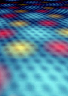
Stacking of graphene sheets

Caption: Stacking of graphene sheets creates regions where the moiré alignment is of type AA (all atoms have neighbors in the layer below), AB (only A atoms have neighbors) or BA (only B atoms have neighbors). In the figure, AA regions are blue-white, while AB and BA regions are red and yellow, respectively.

Credit: Courtesy of Phillip First. Usage Restrictions: None.
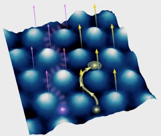
Electron Orbits

Caption: This graphic shows electrons that move along an equipotential, while those that follow closed equipotentials (as in a potential-energy valley) become localized (right). The arrows denote the magnetic field, while hills and valleys are small potential fluctuations.

Credit: Courtesy of Phillip First. Usage Restrictions: None.
"The regular pattern of energy gaps in the graphene surface creates regions where electron transport is not allowed," said Phillip N. First, a professor in the Georgia Tech School of Physics and one of the paper's co-authors. "Electron waves would have to go around these regions, requiring new patterns of electron wave interference. Understanding such interference will be important for bi-layer graphene devices that have been proposed, and may be important for other lattice-matched substrates used to support graphene and graphene devices."

In a magnetic field, an electron moves in a circular trajectory – known as a cyclotron orbit – whose radius depends on the size of the magnetic field and the energy of electron. For a constant magnetic field, that's a little like rolling a marble around in a large bowl, First said.

"At high energy, the marble orbits high in the bowl, while for lower energies, the orbit size is smaller and lower in the bowl," he explained. "The cyclotron orbits in graphene also depend on the electron energy and the local electron potential – corresponding to the bowl – but until now, the orbits hadn't been imaged directly."

Placed in a magnetic field, these orbits normally drift along lines of nearly constant electric potential. But when a graphene sample has small fluctuations in the potential, these "drift states" can become trapped at a hill or valley in the material that has closed constant potential contours. Such trapping of charge carriers is important for the quantum Hall effect, in which precisely quantized resistance results from charge conduction solely through the orbits that skip along the edges of the material.

The study focused on one particular electron orbit: a zero-energy orbit that is unique to graphene. Because electrons are matter waves, interference within a material affects how their energy relates to the velocity of the wave – and reflected waves added to an incoming wave can combine to produce a slower composite wave. Electrons moving through the unique "chicken-wire" arrangement of carbon-carbon bonds in the graphene interfere in a way that leaves the wave velocity the same for all energy levels.

In addition to finding that energy states follow contours of constant electric potential, the researchers discovered specific areas on the graphene surface where the orbital energy of the electrons changes from one atom to the next. That creates an energy gap within isolated patches on the surface.
"By examining their distribution over the surface for different magnetic fields, we determined that the energy gap is due to a subtle interaction with the substrate, which consists of multilayer graphene grown on a silicon carbide wafer," First explained.

In multilayer epitaxial graphene, each layer's symmetrical sublattice is rotated slightly with respect to the next. In prior studies, researchers found that the rotations served to decouple the electronic properties of each graphene layer.

"Our findings hold the first indications of a small position-dependent interaction between the layers," said David L. Miller, the paper's first author and a graduate student in First's laboratory. "This interaction occurs only when the size of a cyclotron orbit – which shrinks as the magnetic field is increased – becomes smaller than the size of the observed patches."

The origin of the position dependent interaction is believed to be the "moiré pattern" of atomic alignments between two adjacent layers of graphene. In some regions, atoms of one layer lie atop atoms of the layer below, while in other regions, none of the atoms align with the atoms in the layer below. In still other regions, half of the atoms have neighbors in the underlayer, an instance in which the symmetry of the carbon atoms is broken and the Landau level – discrete energy level of the electrons – splits into two different energies.

Experimentally, the researchers examined a sample of epitaxial graphene grown at Georgia Tech in the laboratory of Professor Walt de Heer, using techniques developed by his research team over the past several years.

They used the tip of a custom-built scanning-tunneling microscope (STM) to probe the atomic-scale electronic structure of the graphene in a technique known as scanning tunneling spectroscopy. The tip was moved across the surface of a 100-square nanometer section of graphene, and spectroscopic data was acquired every 0.4 nanometers.

The measurements were done at 4.3 degrees Kelvin to take advantage of the fact that energy resolution is proportional to the temperature. The scanning-tunneling microscope, designed and built by Joseph Stroscio at NIST's Center for Nanoscale Science and Technology, used a superconducting magnet to provide the magnetic fields needed to study the orbits.

According to First, the study raises a number of questions for future research, including how the energy gaps will affect electron transport properties, how the observed effects may impact proposed bi-layer graphene coherent devices – and whether the new phenomenon can be controlled.

"This study is really a stepping stone in long path to understanding the subtleties of graphene's interesting properties," he said. "This material is different from anything we have worked with before in electronics." ###

In addition to those already mentioned, the study also included Walt de Heer, Kevin D. Kubista, Ming Ruan, and Markus Kinderman from Georgia Tech and Gregory M. Rutter from NIST. The research was supported by the National Science Foundation, the Semiconductor Research Corporation and the W.M. Keck Foundation. Additional assistance was provided by Georgia Tech's Materials Research Science and Engineering Center (MRSEC).

Contact: John Toon jtoon@gatech.edu 404-894-6986 Georgia Institute of Technology Research News


UCLA chimistes, ingénieurs atteindre le record du monde avec les transistors à grande vitesse graphene

Graphène, un calque d'un atome-une épaisseur de carbone fait, a un potentiel considérable pour faire des appareils électroniques tels que les radios, les ordinateurs et les téléphones plus petits et plus rapides. Mais ses propriétés uniques ont également conduit à des difficultés en intégrant le matériel de ces dispositifs.

Dans un livre publié le 1 septembre dans la feuille de nature, un groupe de chercheurs de l'UCLA démontrer comment ils ont surmonté certaines de ces difficultés pour fabriquer le transistor graphene plus rapide à ce jour.

Avec la mobilité plus élevée de transporteur connus — la vitesse à laquelle les informations électroniques sont transmises par un matériau — graphene est un bon candidat pour radio-fréquence à grande vitesse électronique. Mais les techniques traditionnelles pour la fabrication de matériel souvent entraînent des altérations dans la qualité de l'équipement.
graphene transistors

Illustration de la transistor à grande vitesse graphene conçu par les chercheurs de l'UCLA dirigés par Xiangfeng Duan. Le cylindre dans le milieu du transistor est la porte nanowire rotule.
L'équipe de l'UCLA, dirigée par le professeur de chimie et de la biochimie Xiangfeng Duan, a développé un nouveau processus de fabrication pour transistors graphene à l'aide d'un nanowire comme la porte self-aligned.

Portes Self-Aligned sont un élément clé de transistors modernes, qui sont des dispositifs semi-conducteurs utilisées pour amplifier et de commuter les signaux électroniques.Portes sont utilisés pour passer le transistor entre les différents États et portes self-aligned ont été développés pour faire face aux problèmes d'alignement rencontrées en raison de l'ampleur de rétrécissement de l'électronique.
Pour développer la nouvelle technique de fabrication, Duan associées à deux autres chercheurs de l'Institut de NanoSystems de Californie à UCLA, Yu Huang, professeure adjointe de la science des matériaux et de l'ingénierie au Henry Samueli School of Engineering et spécialisées et Kang Wang, professeur de génie électrique à l'école Samueli.

«Cette nouvelle stratégie surmonte deux limites précédemment rencontrés dans les transistors graphene,» a déclaré Duan."Tout d'abord, il ne produire les défauts éventuels appréciables dans la graphene au cours de la fabrication, donc la mobilité haute transporteur est conservée. Deuxièmement, en utilisant une approche self-aligned avec un nanowire comme la porte d'embarquement, le groupe a pu surmonter alignement précédemment, difficultés rencontrées et fabriquent des périphériques très court-canal avec des performances sans précédent.»

Ces avances permis à l'équipe de démontrer les transistors de graphene de vitesse plus élevés à ce jour, avec une fréquence de coupure jusqu'à 300 GHz — comparables pour les meilleurs transistors de matériaux d'électrons haute mobilité ces arséniure de gallium ou le phosphure d'indium.

«Nous sommes très enthousiastes à propos de notre approche et les résultats, et nous prenons actuellement des efforts supplémentaires à l'échelle de l'approche et de stimuler davantage la vitesse.» a déclaré Lei Liao, fellow postdoctoraux à UCLA.

Radio-fréquence à grande vitesse électronique peut-être également trouver larges applications micro-ondes technologies de communication, d'imagerie et de radar.###

Le financement de cette recherche provenait de la National Science Foundation et le National Institutes of Health.

L'Institut de NanoSystems de Californie à UCLA est un centre de recherche intégrée d'exploitation conjointement à UCLA et UC Santa Barbara, dont la mission est de favoriser les collaborations interdisciplinaires de découvertes nanosystems et nanotechnologies ; former la prochaine génération de scientifiques, des éducateurs et des leaders technologiques ; et faciliter les partenariats avec l'industrie, fueling de développement économique et le bien-être social de Californie, aux États-Unis et du monde.Le CNSI a été créé en 2000 avec 100 millions de dollars à l'état de Californie et un montant supplémentaire de 250 millions de dollars de subventions de recherche fédéraux et le financement de l'industrie.

À l'Institut, les scientifiques dans les domaines de la biologie, chimie, biochimie, physique, mathématiques, computational science et génie sont de mesure, de modification et manipuler les blocs de construction de notre monde — atomes et des molécules.Ces scientifiques bénéficient une culture de laboratoire intégré leur permettant d'effectuer une recherche dynamique à l'échelle du nanomètre, conduisant à des percées importantes dans les domaines de la technologie de la santé, l'énergie, l'environnement et d'informations.

mrodewald@cnsi.UCLA.edu 310-267-5883 , Université de la Californie--Los Angeles


(NanoTechnology)Turning down the noise in graphene

Graphene is a two-dimensional crystalline sheet of carbon atoms – meaning it is only one atom thick - through which electrons can race at nearly the speed of light – 100 times faster than they can move through silicon. This plus graphene's incredible flexibility and mechanical strength make the material a potential superstar for the electronics industry. However, whereas the best electronic materials feature a strong signal and weak background noise, attaining this high signal-to-noise ratio has been a challenge for both single and bi-layers of graphene, especially when placed on a substrate of silica or some other dielectric. One of the problems facing device developers has been the lack of a good graphene noise model.

Working with the unique nanoscience capabilities of the Molecular Foundry at the U.S. Department of Energy (DOE)'s Lawrence Berkeley National Laboratory, a multi-institutional team of researchers has developed the first model of signal-to-noise-ratios for low frequency noises in graphene on silica. Their results show noise patterns that run just the opposite of noise patterns in other electronic materials.
Graphene Noise Patterns

Caption: In the noise models developed at Berkeley Lab's Molecular Foundry, all single layer graphene samples show an M-shaped pattern of noise (top) while all bi-layer graphene samples show a V-shaped noise pattern (bottom). This information will help the development of future graphene devices.

Credit: Image courtesy of Guangyu Xu, UCLA. Usage Restrictions: None.
Berkeley Lab materials scientist Yuegang Zhang led a study in which it was determined that for graphene on silica, the background signal noise is minimal near the region in the graphene where the electron density of states (the number of energy states available to each electron) is lowest. For semiconductors, such as silicon, in the region where electron density states is low the background noise is at its highest. However, there were distinct differences in the noise patterns of single and bi-layer graphene.

"In this work, we present the four-probe low frequency noise characteristics in single- and bi-layer graphene samples, using a back-gated device structure that helps simplify the physics in understanding the interactions between the graphene and the silica substrate," says Zhang. "For single-layer graphene we found that the noise was reduced either close to or far away from the lowest electron density of states, sometimes referred to as the Dirac point for graphene, forming an M-shaped pattern. For the bi-layer graphene, we found a similar noise reduction near the Dirac point but an increase away from that point, forming a V-shaped pattern. The noise data near the Dirac point correlated to spatial-charge inhomogeneity."
The results of this research are reported in the journal Nano Letters in a paper titled "Effect of Spatial Charge Inhomogeneity on 1/f Noise Behavior in Graphene." Co-authoring the paper with Zhang were Guangyu Xu, Carlos Torres Jr., Fei Liu, Emil Song, Minsheng Wang, Yi Zhou, Caifu Zeng and Kang Wang.

Lead author Guangyu Xu, a physicist with the Department of Electrical Engineering at the University of California (UC) Los Angeles, says the spatial charge inhomogeneity responsible for the graphene's unique noise patterns was probably caused by the charge impurities near the graphene-substrate interface.

"Our experiment carefully rules out other possible extrinsic factors that might influence the result," Xu says. "We conclude the correlation between the anomalous noise feature and the spatial charge inhomogeneity, is one of the main carrier scattering mechanisms for unsuspended graphene samples."

Xu says this model of low frequency noise characteristics in graphene should be a significant help for fabricating electronic devices because biasing at the low noise regime can be designed into the device.

"This will benefit the high signal-to-noise ratio in graphene," Xu says. ###

This work was supported in part by DOE's Office of Science.

The Molecular Foundry is one of the five DOE Nanoscale Science Research Centers (NSRCs), national user facilities for interdisciplinary research at the nanoscale, supported by the DOE Office of Science. Together the NSRCs comprise a suite of complementary facilities that provide researchers with state-of-the-art capabilities to fabricate, process, characterize and model nanoscale materials, and constitute the largest infrastructure investment of the National Nanotechnology Initiative. The other NSRCs are located at DOE's Argonne, Brookhaven, Oak Ridge and Sandia and Los Alamos National Laboratories.

Berkeley Lab is a U.S. Department of Energy (DOE) national laboratory located in Berkeley, California. It conducts unclassified scientific research and is managed by the University of California for the DOE Office of Science. Visit our Website at www.lbl.gov.

(NanoTechnology)ORNL scientists help explain graphene mystery

OAK RIDGE, Tennessee, — Échelle du nanomètre simulations et recherches théoriques effectuée à Oak Ridge National Laboratory par le ministère de l'énergie apportent scientifiques plus proche pour réaliser le potentiel du graphene dans les applications électroniques.

Une équipe de recherche menée par de ORNL Bobby Sumpter, Vincent Meunier et Eduardo Cruz-Silva a découvert comment développent des boucles dans graphene, un matériau de faible poids haute résistance électrique conductif qui ressemble à un nid d'abeille à l'échelle atomique.

Les boucles structurelles qui font parfois au cours d'un processus de nettoyage graphene peuvent rendre le matériel inadapté pour les applications électroniques.Surmonter ces types de problèmes est d'un grand intérêt pour l'industrie électronique.

«Graphène est une étoile montante dans le monde de matériaux, compte tenu de son potentiel pour une utilisation dans des composants électroniques précis comme les transistors ou autres semi-conducteurs, a déclaré Bobby Sumpter, un scientifique de personnel au ORNL.
graphene layers

Les simulations ORNL démontrent comment les boucles (vu plus haut en bleu) entre les couches graphene peuvent être réduite à l'aide d'irradiation des électrons (en bas).
L'équipe dynamique moléculaire quantum permettant de simuler un graphene expérimentale, nettoyage de processus, comme expliqué dans un livre publié en lettres d'examen physique.Calculs effectués sur les superordinateurs ORNL a souligné les chercheurs à une étape intermédiaire négligée au cours du traitement.

Imagerie avec un microscope électronique de transmission, ou TEM, soumis le graphene à électrons irradiation, qui finalement a empêché la formation de boucle.Les simulations ORNL a montré qu'en injectant des électrons pour recueillir une image, les électrons changeaient simultanément structure du matériau.
«Prendre une photo avec un TEM n'est pas simplement une photo est prise,» a déclaré Sumpter.«Vous pourriez modifier l'image en même temps que vous cherchez à elle.»

La recherche s'appuie sur les conclusions présentées dans un livre de science 2009 (Jia et coll.), où Meunier et Sumpter aidé démontrer un processus qui nettoie les arêtes graphene en exécutant un courant à travers la matière dans un processus appelé Joule de chauffage.Graphène n'est aussi bon que l'uniformité ou la propreté de ses bords, qui déterminent comment efficacement le matériel peut transmettre des électrons. Meunier, a déclaré la possibilité de nettoyer efficacement les bords graphene est cruciale à l'utilisation de la matière en électronique.

«Imaginez vous disposez d'une voiture de sport fantaisie, mais vous vous rendez compte puis qu'il a roues carrés. Quelle bonne est-il ? C'est comme avoir des bords sur graphene, irréguliers "Meunier dit.

Études expérimentales récentes ont montré que le Joule chauffage processus peut conduire à des boucles indésirables qui se connectent graphene différents calques. Le papier PRL fournit une compréhension atomistique comment électrons irradiation d'un microscope électronique de transmission affecte le processus de nettoyage en empêchant la formation de la boucle de graphene.

«Nous pouvons nettoyer les bords et pas seulement que, nous sommes capables de comprendre pourquoi nous pouvons les, nettoyer» Meunier dit.

L'équipe de recherche inclus des scientifiques du Massachusetts Institute of Technology, Université Catholique de Louvain et Université Carlos III de Madrid.Sumpter et Meunier sont membres de l'informatique et en mathématiques division avec rendez-vous à l'Institut de la théorie des nanomatériaux au sein du Centre des sciences de matériaux Nanophase du ORNL.Cruz-Silva est un chercheur postdoctoral au ORNL.

Partie de ce travail a été appuyé par le Centre pour Nanophase Sciences des matériaux (CNMS) à ORNL.CNMS est l'un des cinq DOE échelle du nanomètre Science Research centres pris en charge par l'Office of Science DOE, installations de premier utilisateur national pour la recherche interdisciplinaire à l'échelle du nanomètre.Ensemble les NSRCs comprennent une suite d'installations complémentaires qui fournissent des chercheurs avec capacités de-la-pointe à fabriquer, processus, caractérisent et modéliser les matériaux de l'échelle du nanomètre et constituent le plus grand investissement dans l'infrastructure de l'initiative nationale de la nanotechnologie.Les NSRCs sont trouvent en Argonne du DOE, Brookhaven, Lawrence Berkeley, Oak Ridge et Sandia Los Alamos laboratoires nationaux.Pour plus d'informations sur les NSRCs DOE, visitez http://nano.energy.gov.ORNL est géré par UT-Battelle for Office de la science par le ministère de l'énergie.

Avec les médias : Morgan McCorkle Communications et relations de 865. 574. 7308