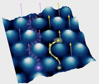
In the Aug. 8 advance online edition of the journal Nature Physics, researchers from the Georgia Institute of Technology and the National Institute of Standards and Technology (NIST) describe for the first time how the orbits of electrons are distributed spatially by magnetic fields applied to layers of epitaxial graphene.
The research team also found that these electron orbits can interact with the substrate on which the graphene is grown, creating energy gaps that affect how electron waves move through the multilayer material. These energy gaps could have implications for the designers of certain graphene-based electronic devices.
In multilayer epitaxial graphene, each layer's symmetrical sublattice is rotated slightly with respect to the next. In prior studies, researchers found that the rotations served to decouple the electronic properties of each graphene layer.
"Our findings hold the first indications of a small position-dependent interaction between the layers," said David L. Miller, the paper's first author and a graduate student in First's laboratory. "This interaction occurs only when the size of a cyclotron orbit – which shrinks as the magnetic field is increased – becomes smaller than the size of the observed patches."
The origin of the position dependent interaction is believed to be the "moiré pattern" of atomic alignments between two adjacent layers of graphene. In some regions, atoms of one layer lie atop atoms of the layer below, while in other regions, none of the atoms align with the atoms in the layer below. In still other regions, half of the atoms have neighbors in the underlayer, an instance in which the symmetry of the carbon atoms is broken and the Landau level – discrete energy level of the electrons – splits into two different energies.
Experimentally, the researchers examined a sample of epitaxial graphene grown at Georgia Tech in the laboratory of Professor Walt de Heer, using techniques developed by his research team over the past several years.
They used the tip of a custom-built scanning-tunneling microscope (STM) to probe the atomic-scale electronic structure of the graphene in a technique known as scanning tunneling spectroscopy. The tip was moved across the surface of a 100-square nanometer section of graphene, and spectroscopic data was acquired every 0.4 nanometers.
The measurements were done at 4.3 degrees Kelvin to take advantage of the fact that energy resolution is proportional to the temperature. The scanning-tunneling microscope, designed and built by Joseph Stroscio at NIST's Center for Nanoscale Science and Technology, used a superconducting magnet to provide the magnetic fields needed to study the orbits.
According to First, the study raises a number of questions for future research, including how the energy gaps will affect electron transport properties, how the observed effects may impact proposed bi-layer graphene coherent devices – and whether the new phenomenon can be controlled.
"This study is really a stepping stone in long path to understanding the subtleties of graphene's interesting properties," he said. "This material is different from anything we have worked with before in electronics." ###
In addition to those already mentioned, the study also included Walt de Heer, Kevin D. Kubista, Ming Ruan, and Markus Kinderman from Georgia Tech and Gregory M. Rutter from NIST. The research was supported by the National Science Foundation, the Semiconductor Research Corporation and the W.M. Keck Foundation. Additional assistance was provided by Georgia Tech's Materials Research Science and Engineering Center (MRSEC).
Contact: John Toon jtoon@gatech.edu 404-894-6986 Georgia Institute of Technology Research News


No comments:
Post a Comment